Design and prototyping
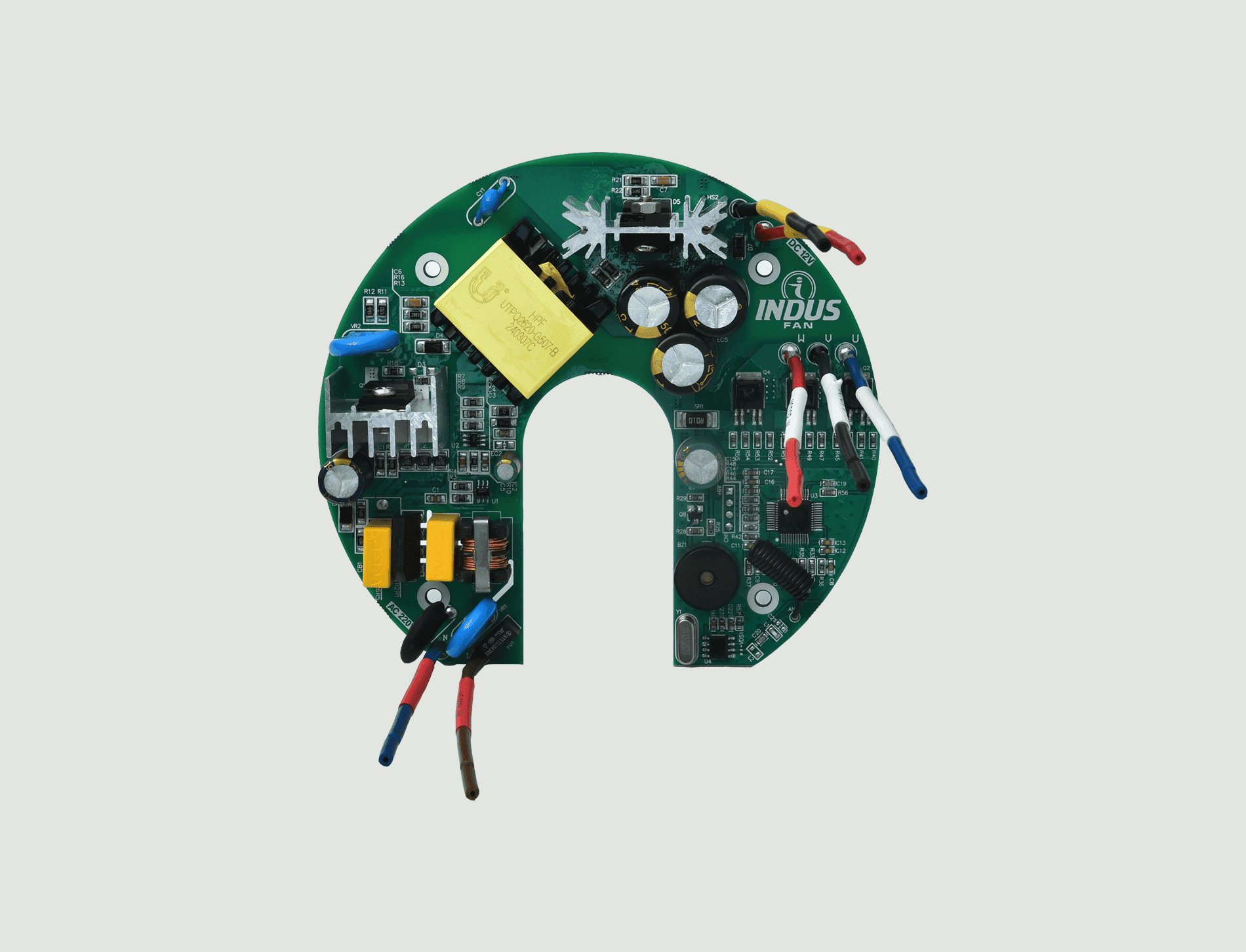
PCB layout and component-placement planning based on electrical and mechanical requirements.

Expertise
Surface-mount assembly workflow from PCB design and solder-paste printing through component placement, reflow, inspection, testing and rework.
UT / POWER ELECTRONICS
Surface-mount assembly workflow from PCB design and solder-paste printing through component placement, reflow, inspection, testing and rework.
Scope
PCB layout and component-placement planning based on electrical and mechanical requirements.
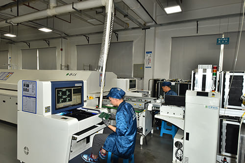
Application of solder paste to the PCB through a stencil.
Automated pick-and-place equipment positions SMT components on the board.
Controlled heating forms electrical connections between components and PCB pads.
AOI and electrical testing are used to detect placement, soldering and functional defects.
Defective components or solder joints can be corrected before the next assembly stage.
Connected delivery
Use the contact channel to connect this capability to a product model, prototype or production requirement.
Browse productsStart a conversation
Include the application, development stage, production scope and available technical requirements.
Get in touch